5 Analysis of Design
5. 1 Problem
Here is a section of source code analysis. An example analysis was performed
using trace mode-2 in Veritak Simulator. (Off course, you can use
another tool).
Load Veritak Project "altera_rtl_trace_count.vtakprj"
Let's look at the instruction "ori $sp,$sp,#$3380". Micro operation
is
| $sp | #$3380 => $sp |
|---|
It is noted that Register File $sp has not been written yet even at Stage5.
What will be happened if $sp is referenced in any stage of stage2-stage5
? This is called RAW (Read After Write) Data Hazard.
Forwarding mechanism overcomes this problem.
| Time Slot | Stage1 | Stage2 | Stage3 | Stage4 | Stage5 |
|---|---|---|---|---|---|
| Set Register File Address | Read Register File ALU_LEFT/Right Latch |
Mem Write AReg<=ALU |
Mem Read NReg<=AReg |
Write Register File RReg<=NReg |
|
| 1 | Fetch & Decode ori $sp,$sp,#$3380 |
||||
| 2 | Fetch & Decode sw $z0,0($a0) |
ReadRegisterFile ALU_LEFT<=0 ALU_RIGHT<=#$3380 |
|||
| 3 | Fetch & Decode slt $v1,$a0,$a1 |
ReadRegisterFile | ALU=LEFT(0) or RIGHT(#$3380); AReg<=ALU |
||
| 4 | ReadRegisterFile | ALU | NReg<=AReg | ||
| 5 | ALU | MEM | WB Register FieAddres=$sp Write Data=#$3380 |
||
| 6 | MEM | WB | |||
| 7 | WB | ||||
| 8 |
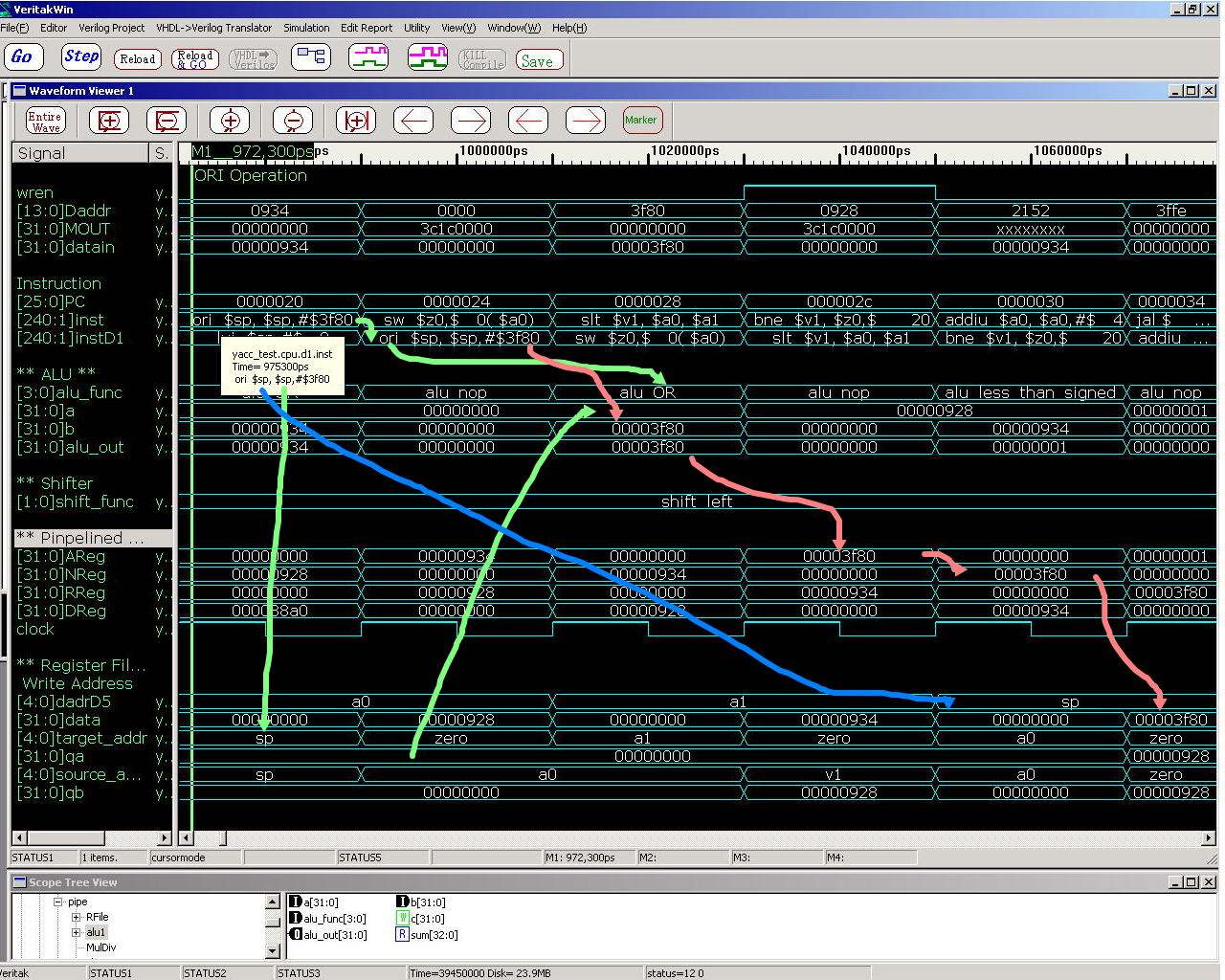
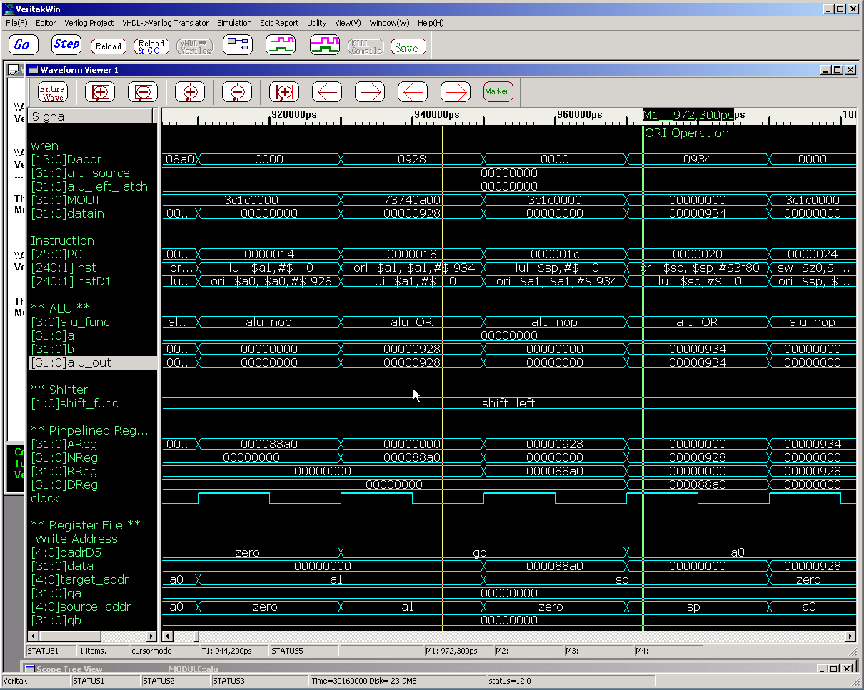
5.2 "Forwarding" Analysis
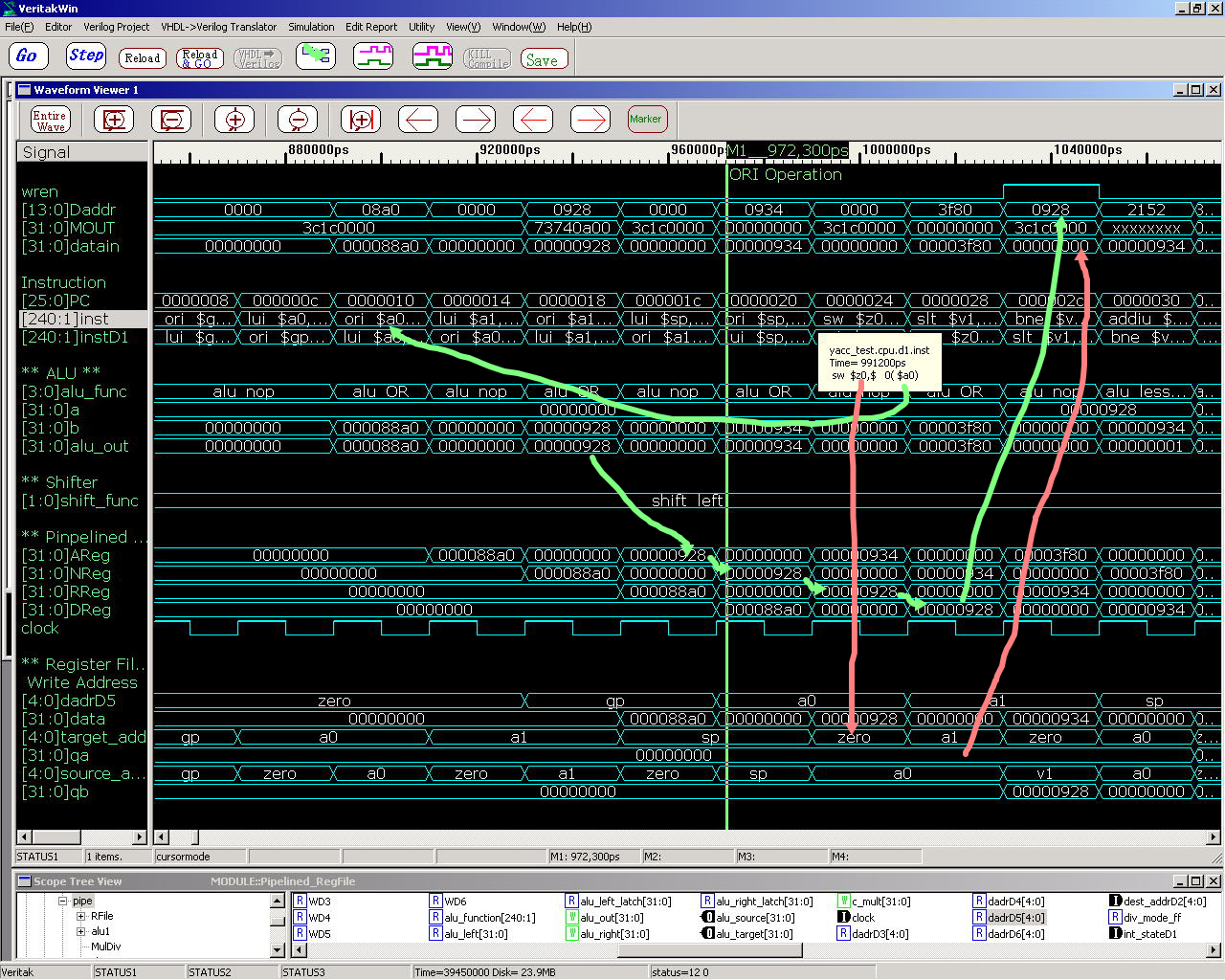
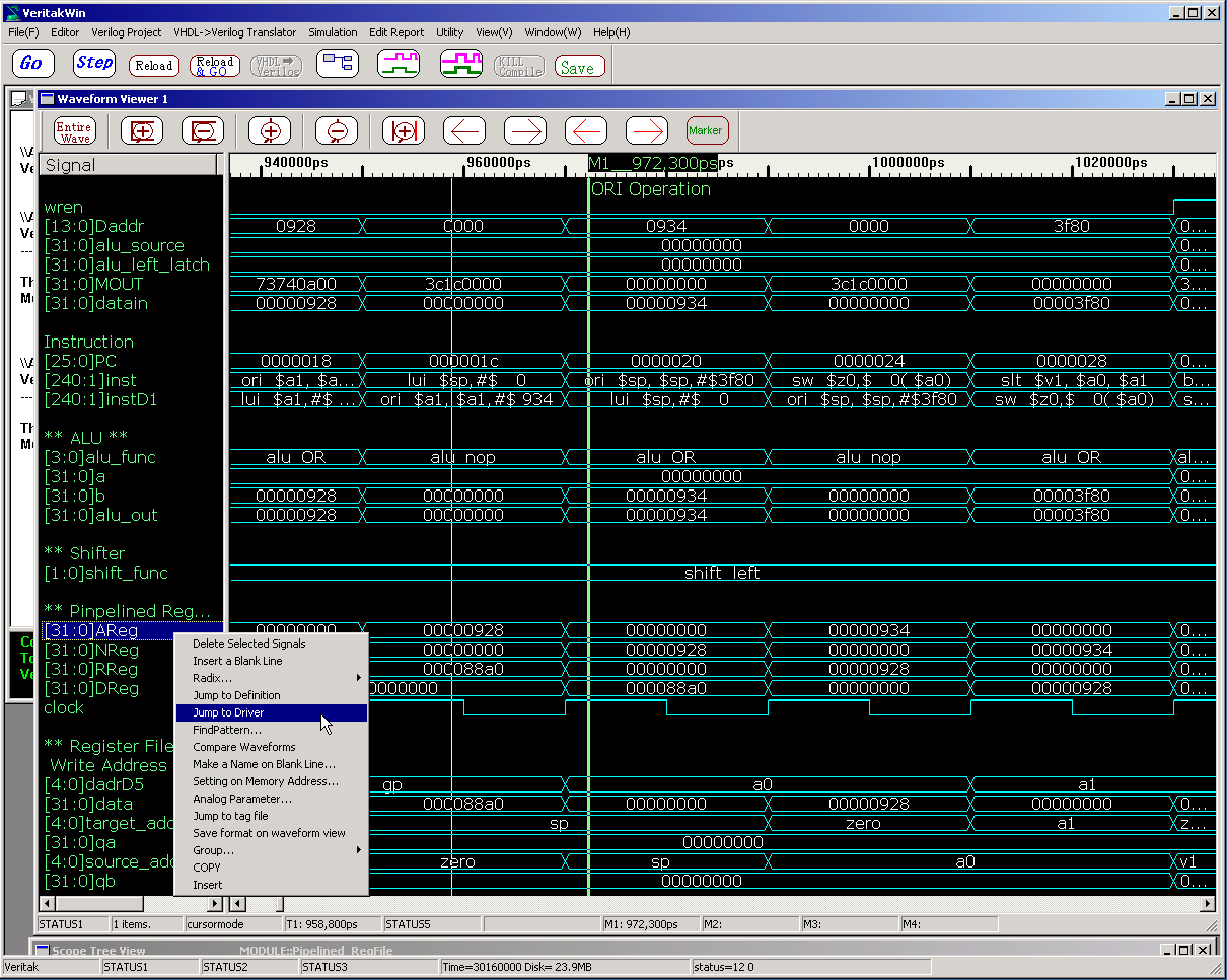
Let's look at tool-tip displays "sw $z0, 0($a0)"
This instruction causes RAM Write operation at the address of 0x928 followed
by 2 clocks. However, 0x928(=$a0) has been set by the instruction ori $a0,$a0,0x928
prior to 5cycles. So this is the forwarding case.
Pipelined Registers carry 0x928 in forwarding.
Let' trace the situation back in following analysis.
|
0: 3c1c0000 lui $gp,0x0 |
|---|
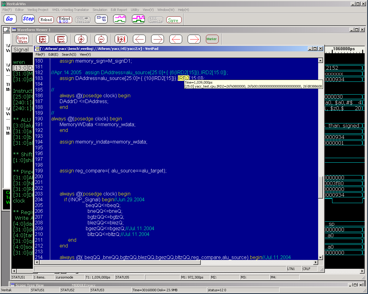
To investigate what is driving the Daddress 0x928, Jump to tag file,
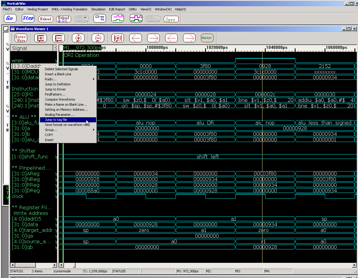
Then jump to the tag file which describes entire structure of design by
text file.
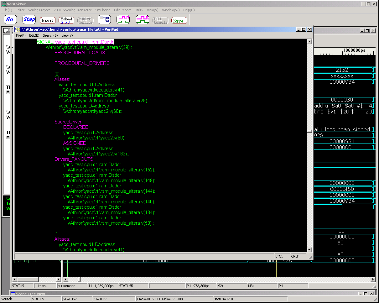
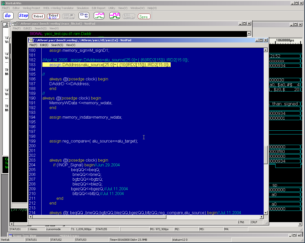
Move to SourceDriver =>Assigned:
Select the signal,and DBLCLICK
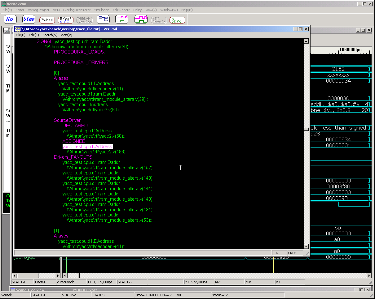
Jumps to the source code where DAddress is assigned.
We realize that DAddress is result of ( not time consuming) add operation
between alu_source and IRD2 concerned.
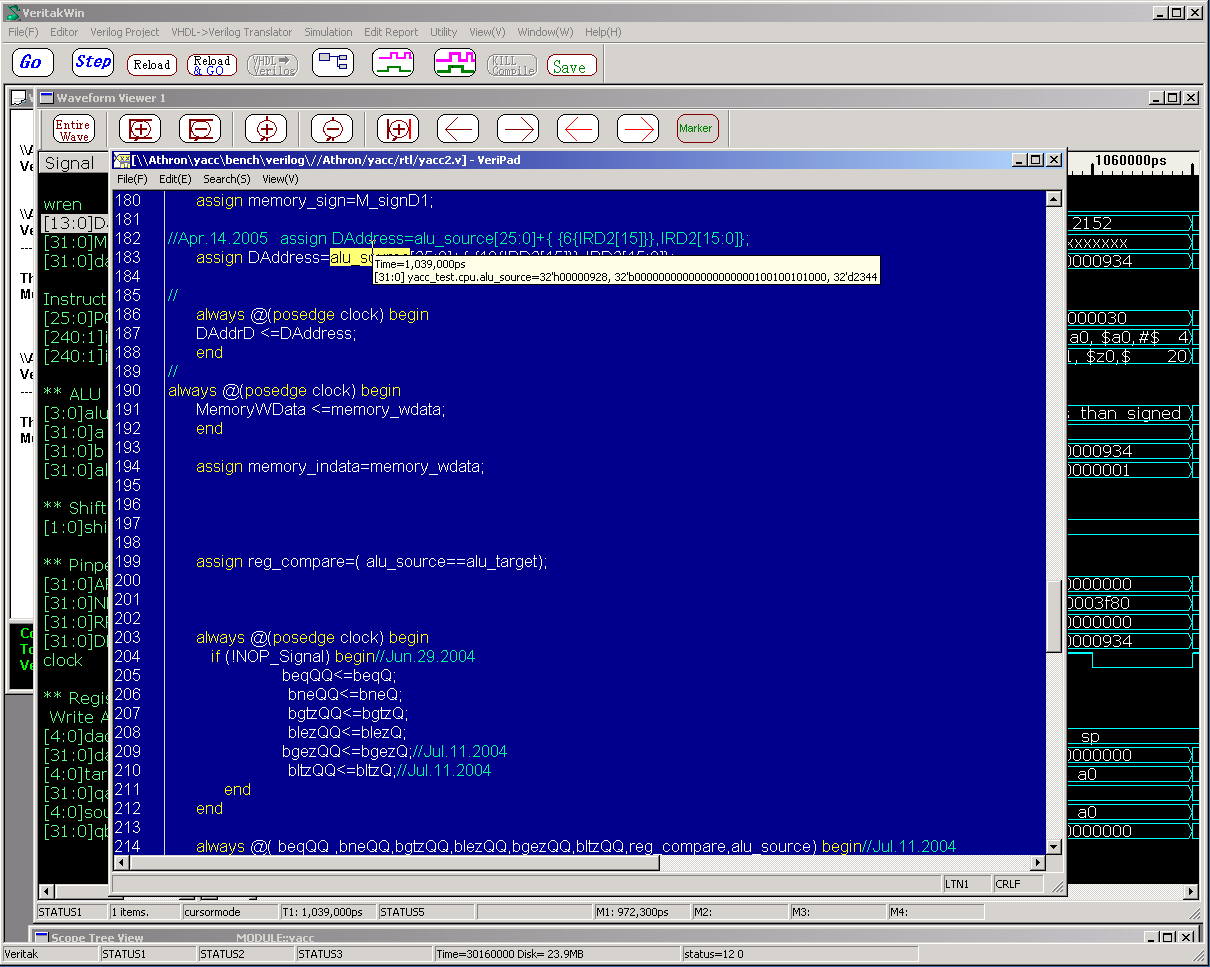
There is another way to jump to the driver.
You can jump to the source code by "Jump to Driver" directly.
Set T1 cursor at write strobe time, select the signal ,and Jump to Driver..
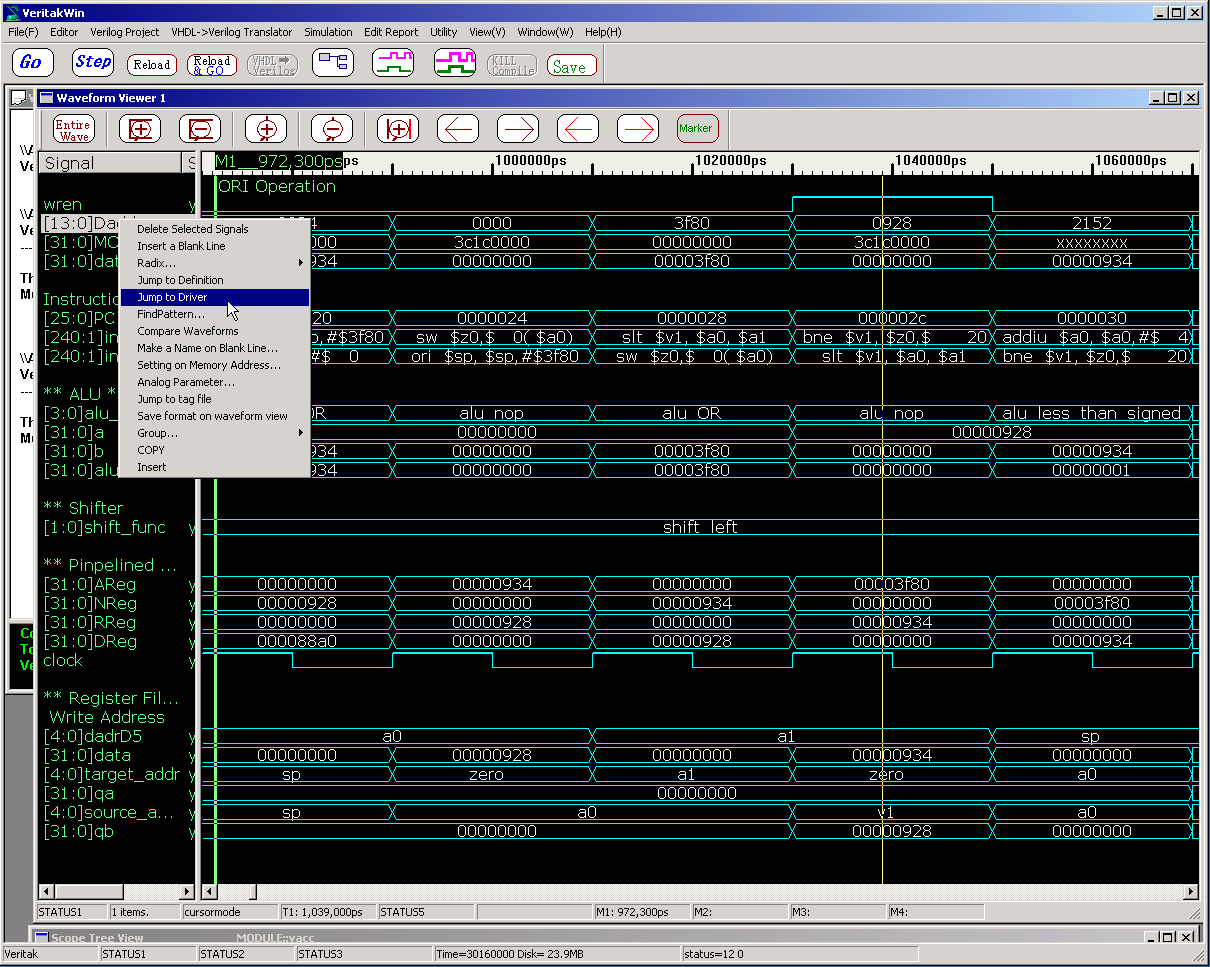
Same result as tag-jump.
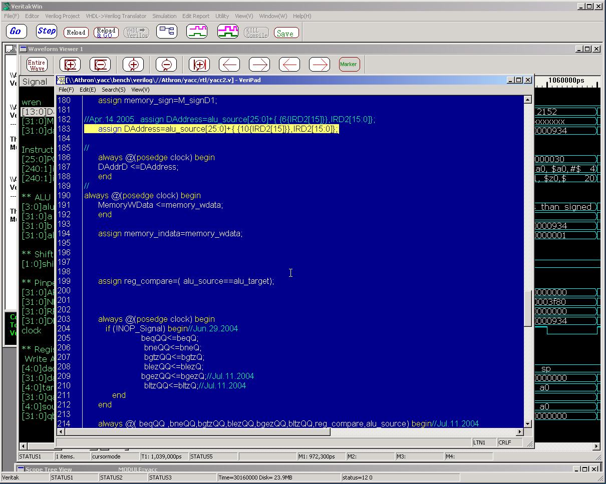
Since this assignment is combinational logic, you can view the value by
tool tip.
Now, we realize that "alu_source" is 32'h928 which is next target
for further analysis.
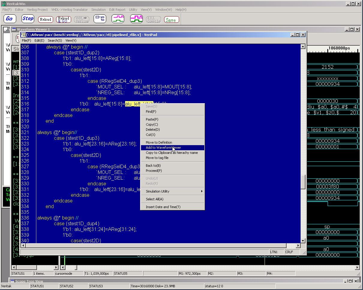
Add "alu_source " to WaveformView for further analysis.
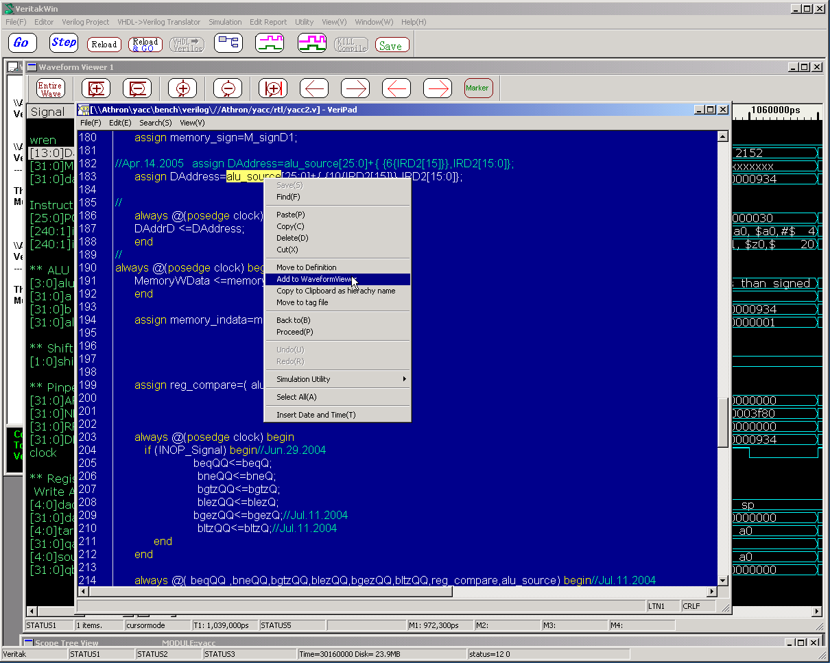
Jump to Driver for "alu_source"
Warning Displayed.
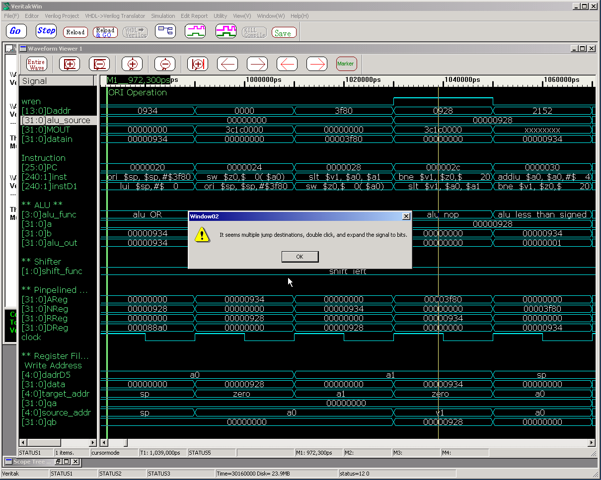
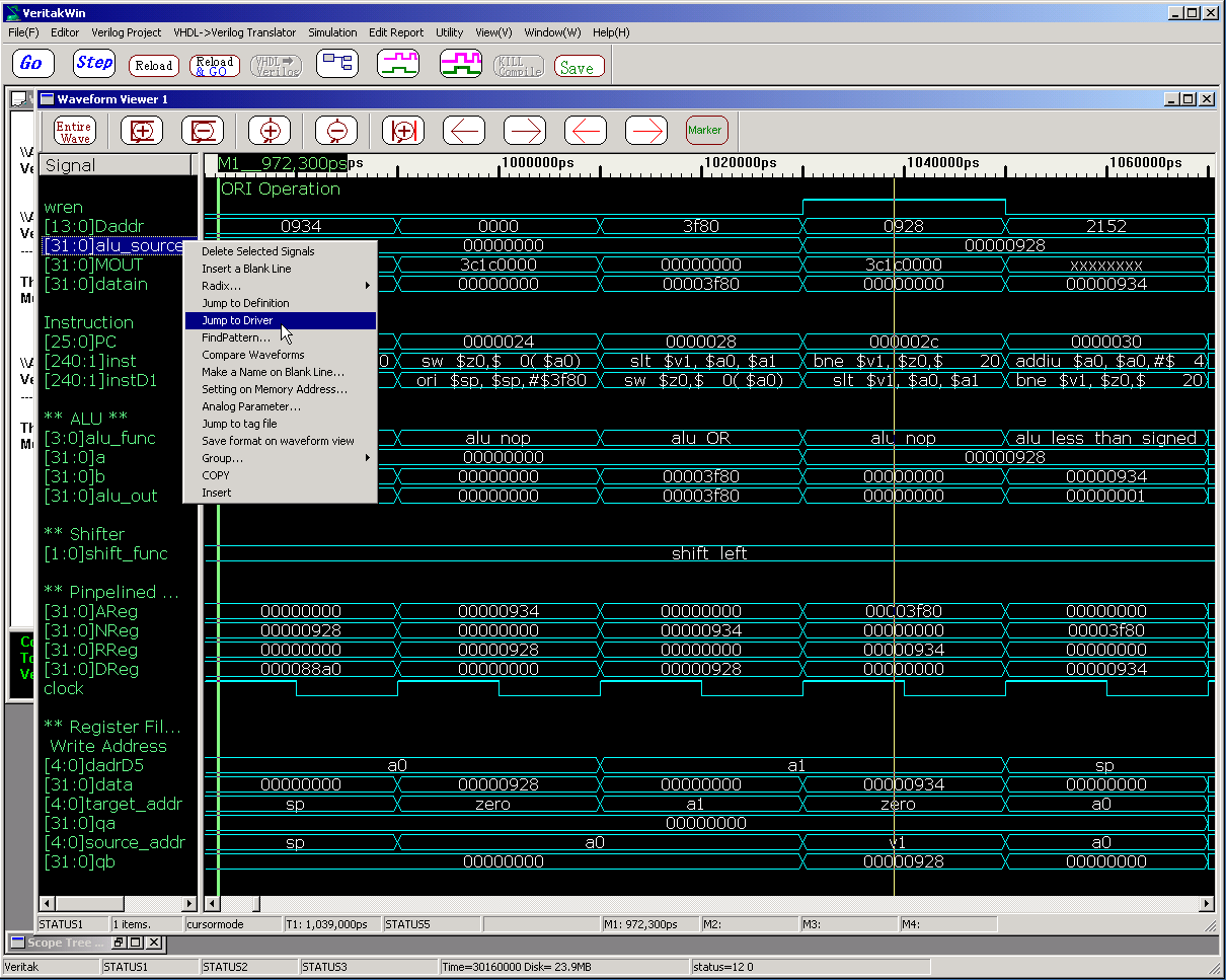
Expand the signal to bits.
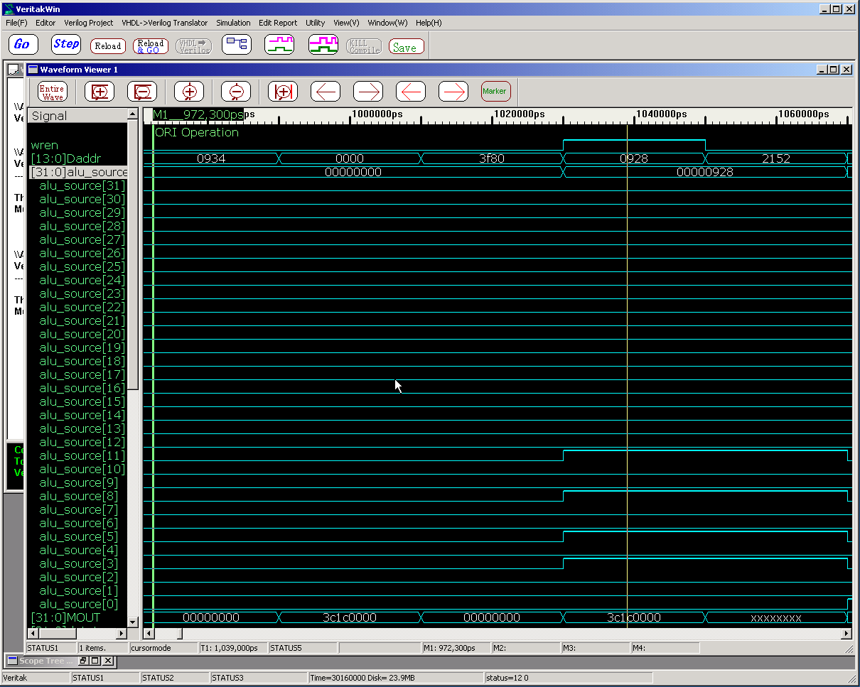
Then jump to driver by any signal activated.
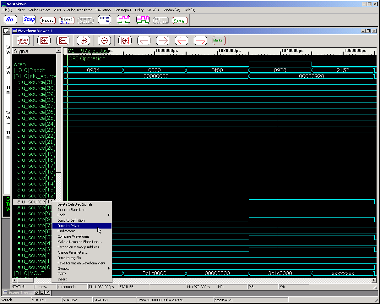
Then jumps to the position. This is combinational circuit which has no
time-consumption. We can tool-tip the value in this case.
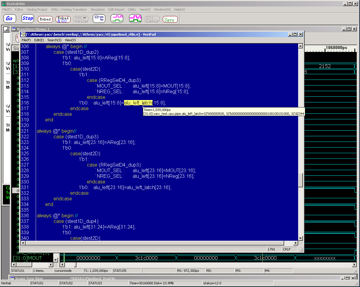
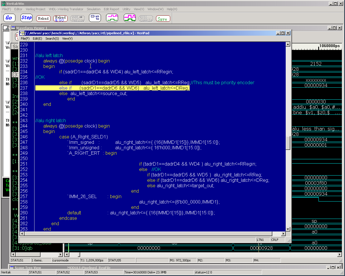
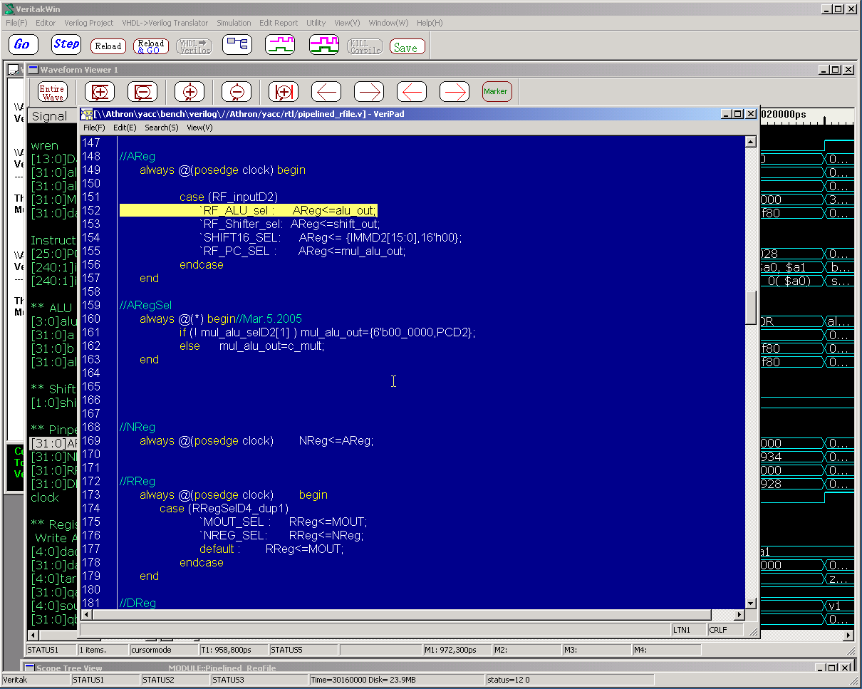
Add "alu_left_latch " to the WaveformView for further analysis.
Jump to Driver..
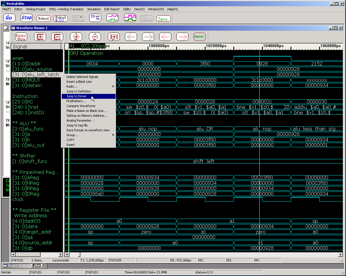
Jumps to the position where "alu_left_latch" is assigned by non-blocking
statement
Jump to Driver by "DReg" at T1 cursor.
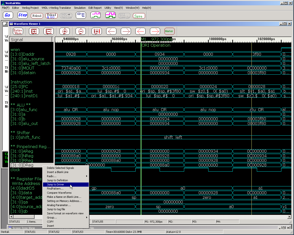
We realize "DReg " is just pipelined register
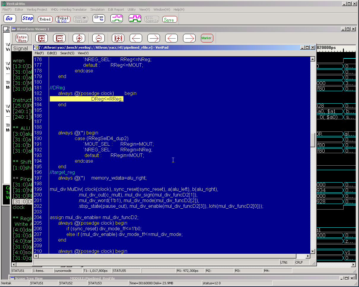
Let's investigate what is driving "RReg".
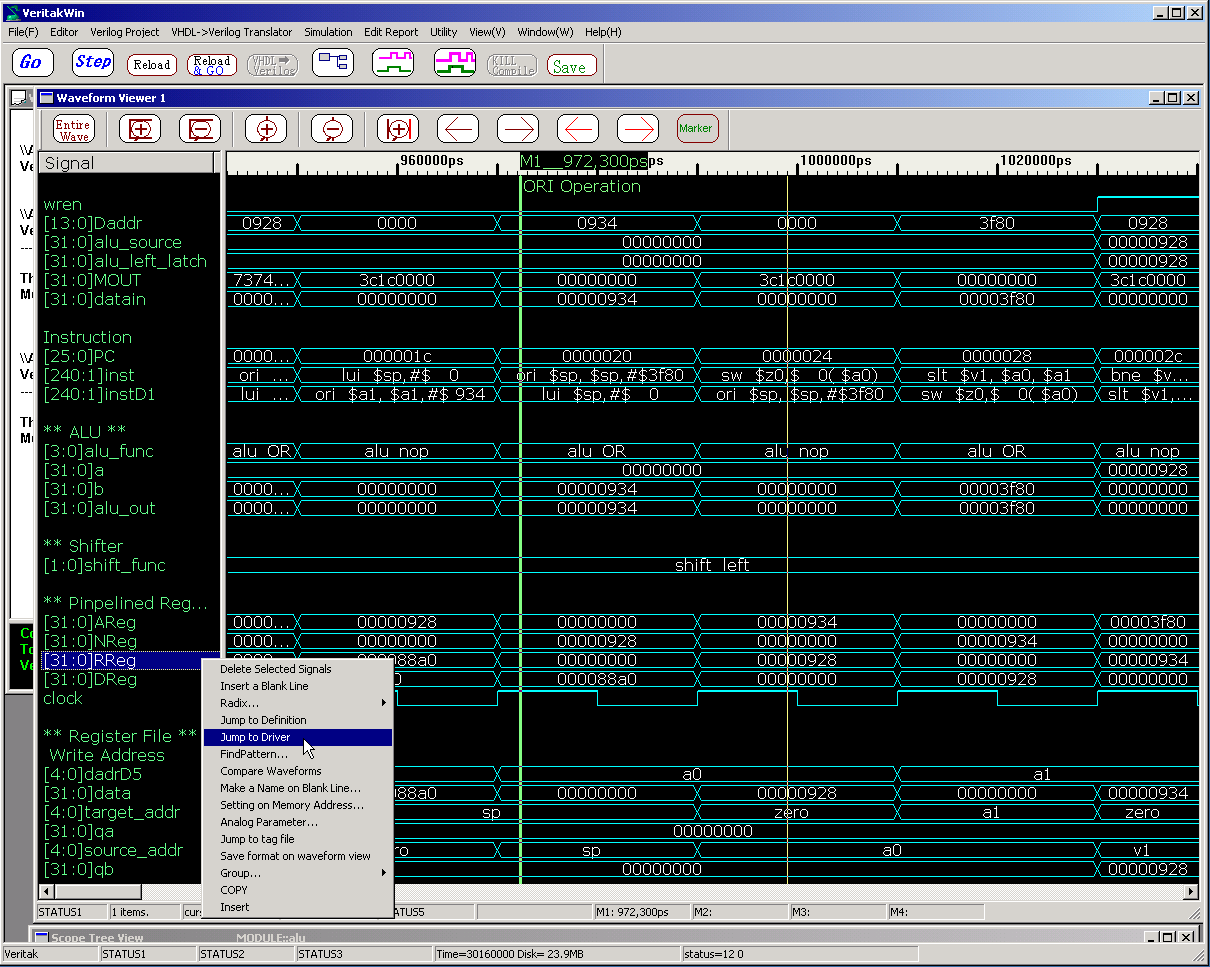
NReg is Driving.
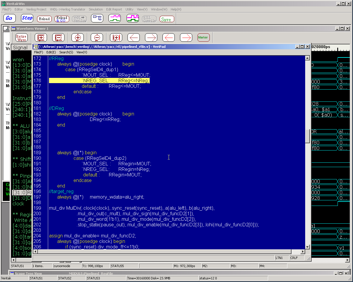
What is driving "NReg" ?
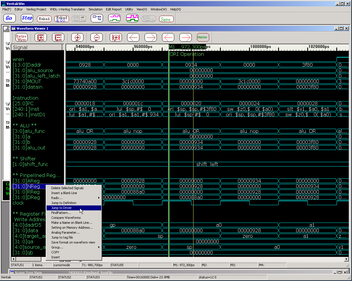
"AReg" is driving.
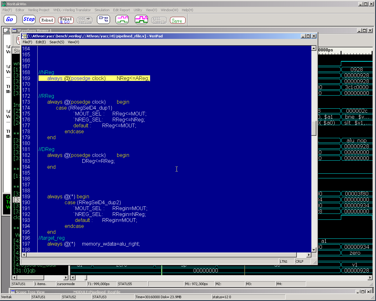
What is driving "AReg"?
"alu_out " is driving.
Then investigate the driver of "alu_out".
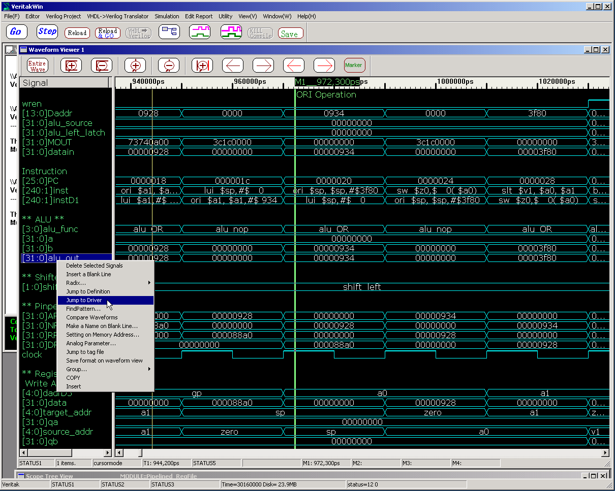
We realize alu_out=a | b;

Finally We understand "the value 0x928 is derived from the instruction
" ori $a0, $a0,#$928" through pipelined registers ,not from register
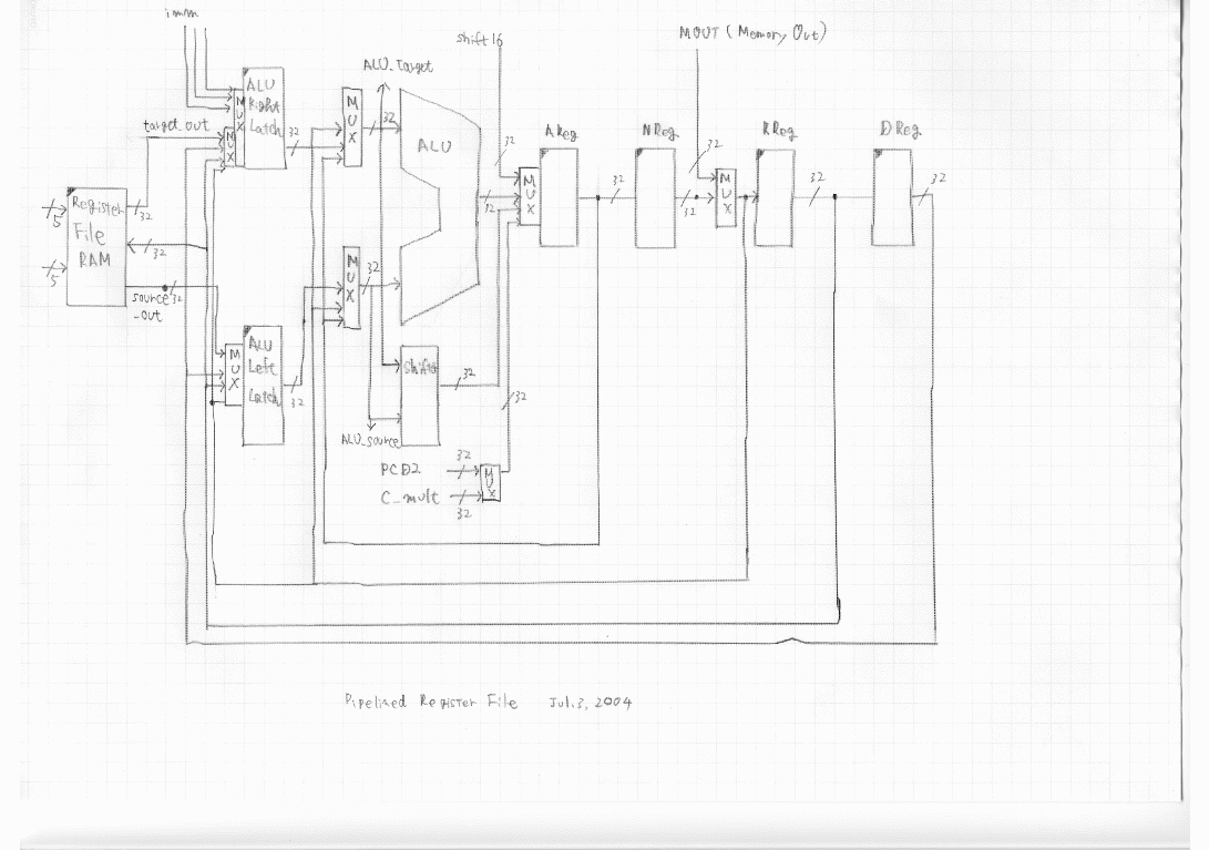
file's output. You can see block diagram I wrote ,which is a sketch in early design stage.